Fast PCB

Technologies

Design parameters

  • Layout Scale Max.
    90000 pins +
  • Layer Count Layout Max.
    42
  • BGA Quantity
    100 +
  • Line/Space Min.
    1.9 mil
  • Hole Diameter Min.
    6 mil (Mechanical Drilling) / 4mil (Laser Drilling)
  • BGA Pitch
    0.30 mm
  • BGA Pins Max.
    3647 pins
  • Signal Transmission Speed Max.
    56G

Main chips involved

  • Processor
    Intel: Purley Haswell platform Ivy Bridge and Sandy Bridge Series Shark Bay Mobile Platform
    Marvell: PXA920/920H Series Xelerated series ARM ADA1000/1500 98CX8129/8297
    Qualcomm/SPRD/MTK Mobile: MSM86XX / 82XX / 76XX SC9610 / 8810 / 6820 MT6573 / 6575 / 6577/ 6589
    Freescale PowerPC Series: MPC8541 / 8548 / 8555 / 8641 P2020
    TI: AM35X / 38X OMAP4430 / P3505 66AK2EX C667X TMX320C
    ADI: TS101/201 ADUCM3027/3029
  • FPGA / CPLD
    AMD/Xilinx: Spartan-6 Spartan®-6 Artix-7 Kintex-7 Virtex-7 Virtex-ultrascale Virtex5 Zynq-7
    INTEL/Altera: Stratix Series Arria Series Cyclone series MAX Series
    Cavium: CN7XXX CN6XXX NITROX III NITROX PX CN50XX SC9610 / 8810 / 6820 MT6573 / 6575 / 6577/ 6589
    Lattice: MachX03 Series MachX02 Series
  • Memory Chip
    Samsung: DDR4 DDR3 DDR2
    Hynix: DDR4 DDR3 DDR2
    Elpida: DDR3 DDR2
    Mircon: DDR4 DDR2 DDR3
    Cypress: CY7C1510 CY7C1565 CY7C25XX

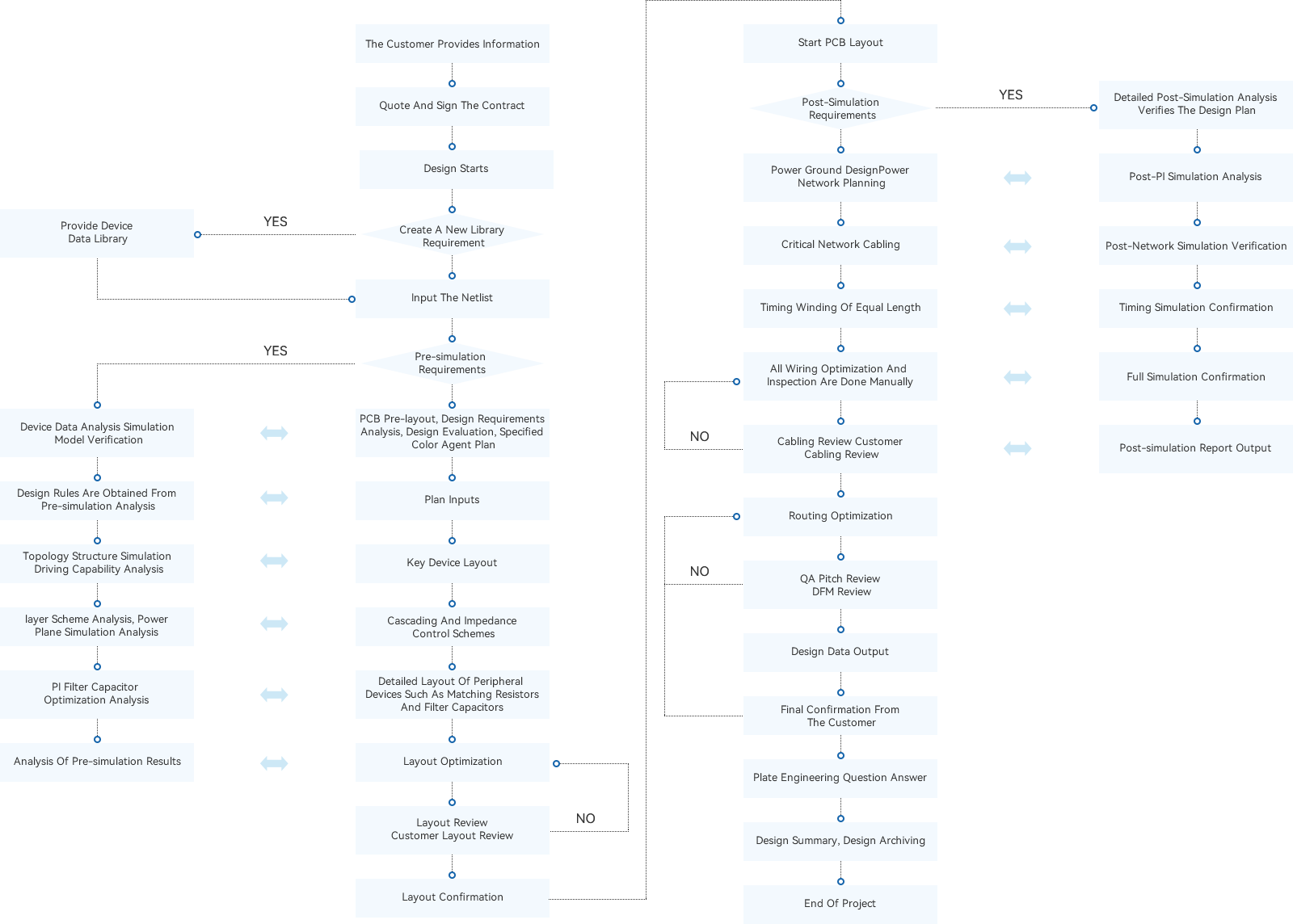
Design process

Introduction to Simulation

    Signal integrity analysis
    Design rules, topology pre-imitation
    Reflection, crosstalk, timing analysis
    Multi-plate joint system analysis
    Support IBIS model, Hspice model and S-parameter model frequency domain,time domain, channel multiple simulation analysis methods, to ensure high-speed transmission performance comprehensive consideration of reflection, crosstalk, ringing, eye diagram, jitter, bit error rate, S-parameter DDR3, DDR3L, DDR4, PCIE, Serdes, SFP+ a large number of simulation cases, with rich practical experience
    Main simulation analysis projects
    Delay Caculate Topology analysis
    Reflection Impedance Cal
    Cross talk Stack up
    Static timing analysis SSN simulation
    S-parameter Serial Parallellink
    DC Voltage Drop Analysis
    Planar Resonance Analysis
    PDN Impedance Analysis
    Optimization Analysis of Decoupling Capacitor
    EMC Analysis
    EMC Design
    EMC Rectiification
    EMC Testing
    Electromagnetic compatibility includes electromagnetic interference EMC and electromagnetic sensitivity EMC. The board level EMC design adopts the idea of focusing on source control, taking countermeasures from the beginning of the design phase, and combining Signal integrity analysis, fundamentally solving the EMC problem. In boards with external interfaces and products that cannot be fully shielded, board level EMC design cannot be replaced by any other EMC measures. The consideration of EMC design in the aspect of single boards will reduce the pressure on subsequent processes and shorten the development cycle to reduce batch production costs.
    EMC Design
    Stacking and impedance control
    Module division and special device layout
    Priority wiring for power and special signals
    Cross partition and slot design
    Interface protection and filtering design
    Ground separation and connection, shielding and isolation
    EMC Rectification
    Propose rectification plans for the issues identified during EMC testing of customer products, mainly starting from factors such as interference sources, sensitive devices, and coupling pathways. Based on actual testing and performance issues, propose rectification suggestions and carry out rectification.
    EMC Testing
    Assist customers in completing a series of electromagnetic compatibility tests for their products and provide reference suggestions for any issues encountered. EMC testing laboratories can be provided, greatly reducing customer development time and costs.
    DFx Analysis
    DFF -  Design For Fabrication
    DFA -  Design For Assembly
    DFT -  Design For Testing
    Design for Manufacturability (DFM) is the process of considering factors such as manufacturability and assemblability during the design phase, in order to manufacture a product with the lowest cost, shortest time, and highest quality.
    Advantage
    Reduce the number of revisions, shorten the development cycle Reduce trial production times, and reduce production costs
    Improve standardization process, improve product quality and reliability Simplify product conversion process, and increase productivity